![[CS Dept logo]](/images/logos/cs-dept-logo.gif)
![[CS Dept logo]](/images/logos/cs-dept-logo.gif)
![[back]](http://cs-www.uchicago.edu/images/logos/UofCsealTiny.gif) Department of Computer Science
Department of Computer Science
![[]](http://cs-www.uchicago.edu/images/logos/UofCsealTiny.gif) The University of Chicago
The University of Chicago
Last modified: Sun Jan 4 21:10:42 CST
These notes give a very superficial introduction to the electronics of digital VLSI (Very Large Scale Integration). The object is to give you
For present purposes, you don't need to understand electronics or electromagnetic physics in any sort of detail. There are two physical quantities that are crucial to electronics: voltage and current. If you don't know any electronics, think of electrical charge as a gas (like the air). Wires are like pipes. Imagine that voltage is a lot like pressure, and that current is a lot like the rate of flow of the gas. Strictly speaking, voltage is measured as a difference in electrical potential between two points. Just as there is a standard air pressure at sea level, there is a standard ground voltage, which is taken as a convenient 0 for the scale. Most of the world around us is at this neutral ground voltage. The voltage of a single point in an electronic system is the difference between that point and some point with ground voltage. Current may be measured through any 2-dimensional surface, but normally we consider the current through some cut in a wire. Except for certain rapid transient effects, the current in a continuous segment of wire is the same at every cut.
Every path through an electronic system has a certain resistance to electrical current. The current from point a to b along a path p is the voltage difference between a and b, divided by the resistance along p.
A material with very low resistance is called a ``conductor,'' and a material with very high resistance is called an ``insulator.'' The meanings of ``very low'' and ``very high'' depend on the context. In any given electronic system, an insulator is essentially a material that will never carry a noticeable current. A conductor is a material that cannot sustain a noticeable voltage difference. In most contexts, copper, silver, gold are good conductors, and glass is a good insulator. Air is usually considered an insulator, but in thunderstorms it is sometimes considered a conductor, because the electrical energy in a thunderstorm is so high.
Some materials can be made to act variously as insulators or conductors by small changes, such as the introduction of impurities, or the presence of an electrical charge nearby. Such materials are called ``semiconductors,'' and silicon is one such material. Small variations in the material structure of silicon, including introduction of slight impurities, can vary it between an insulator and a good conductor. In some forms of silicon, a small electrical charge near the material can control its conductive/insulating properties. In principle, all of these variations are just changes in resistance, but we can get a qualitative idea of VLSI circuitry by thinking of most of them as changes between insulator and conductor.
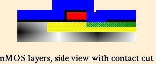
VLSI circuitry starts with a smallish piece of silicon, called a ``wafer,'' and introduces layers of other material on different parts of the silicon surface. There is a variety of VLSI fabrication techniques, each with different properties for digital circuit design. I will talk about a common technique, called ``nMOS,'' just because I know it best. Other common techniques include CMOS and HMOS, and you may read about them elsewhere.
The underlying silicon in an nMOS wafer acts as an insulator. But, in the presence of an electrical charge very near the surface, it can conduct. There are two types of impurities that are diffused (``doped'') into the silicon.
The order in which the doping, layering, and cutting are done is very important:

A transistor is an electronic component with three connections, called the ``source,'' ``drain,'' and ``gate.'' A relatively small voltage on the gate controls the resistance between source and drain, which can produce a substantially larger voltage or a current there. In nMOS transistors, the source and drain are indistinguishable, but in some transistors they behave differently.
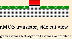
On an nMOS wafer, wherever a red polysilicon wire crosses a green
wire, there is a transistor. The red is the gate, and the greens on
either side are source and drain. The green doping is applied all the
way across the red wire, but Because the red layer is laid before the
green doping, the green doping is blocked and it does not
actually extend under the red wire. This trick is important, since it
produces a very accurate placement of the boundary of the green doping
at the edge of the red wire. Here is a side view of a typical nMOS
enhancement mode transistor.

In nMOS circuits, Boolean 0s are represented by voltages near numerical 0 (ground). There is another special voltage, called VDD (the two Ds are subscripts, but I haven't yet generated an image for that symbol: look on the picture in the next section), and voltages near VDD represent Boolean 1s. The normal design style in nMOS circuits uses lots of parallel blue metal wires carrying VDD voltage, interleaved with parallel blue metal wires carrying ground voltage. The computing action takes place in the green and red layers between these metal wires.
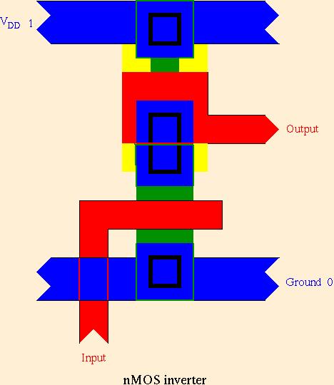
Here is a picture from the top of a region of silicon acting as an
nMOS invertor.

The left-right blue wire at the top must be connected to a voltage source providing VDD. The other left-right blue wire at the bottom must be connected to the ground voltage. The input to be inverted comes in on the red wire from the bottom, which crosses under the blue ground wire with no connection. There is a broad green area going up from a contact cut with the blue ground wire. Where the red input crosses this green region, we get an enhancement mode transistor. A voltage significantly higher than ground on the input (representing a Boolean 1) connects the green regions above and below the red input, so the middle of the circuit is pulled close to the ground voltage (Boolean 0). This lower transistor is called the ``pulldown'' transistor. The contact cut in the middle connects the upper part of the pulldown transistor to the red wire in the middle, which feeds off to the right as the output. So, it's pretty clear that a 1 input should produce a 0 output.
The behavior on 0 input is a bit trickier. The mess between the middle and upper contact cuts is a depletion mode transistor, called the ``pullup.'' The yellow doping extends under the red, though you can't see it in the picture. If depletion mode transistors had nice behavior symmetric to enhancement mode, we might use the input to gate this upper transistor, too. Instead, the gate voltage for the upper transistor is connected directly to its drain, through the middle contact cut. In this configuration, the depletion mode transistor acts essentially like a resistor. When input is 0, there is essentially no current through the pullup, because there's nowhere for it to go from the middle contact cut (the red output leads to another dead end somewhere). So, the output voltage in the middle is very close to VDD, representing Boolean 1.
Notice that, on input 1, there is a noticeable current from top to bottom, sufficient to induce a voltage near VDD across the pullup.
The invertor is very important, partly because its negative behavior is relatively unusual in electronic components, but also because it incorporates an amplifier. The voltage on the input can be much smaller than VDD and still activate the pulldown transistor. A pair of invertors, connected in sequence, can be used to amplify a Boolean value without inverting its sense. To some extent, or operations may be implemented simply by joining wires, but this gradually weakens the signal, and it is important to go through invertors regularly to maintain the strength of the signal. Long wires may also require invertors along the way. Because of the electronic importance of invertors, nMOS and similar circuit techniques are sometimes called ``invertor logic.''
The strength of the output signal (not just its voltage, but its ability to drive lots of additional circuitry without degrading that voltage too much) is essentially determined by the width of the green region in the pulldown transistor. I have shown it twice the minimum width of a green wire, but it is often 3 or 4 times as wide.
The basic idea of a nor gate is a pretty simple
generalization of an invertor. Merely connect several pulldowns, with
independent gate inputs, to the same pullup and output. Except for
balancing the detailed electronic properties of pulldowns, pullup, and
the circuits driven by the output, that's all there is too it. Here's
a picture of a binary nor.

In principle, all gates may be built from nors. In practice, particular functions often have more efficient specialized implementations in VLSI circuitry. The precise shape of a VLSI circuit depends on the additional circuitry driven by its output, and on speed and power considerations, as well as the Boolean functionality.
The principles of nMOS, and other types of VLSI, have been cooked into formal rules dealing with the width required for pulldowns in various contexts, the gaps required between various sorts of wires, etc. These rules aren't trivial, but anyone can learn them in a quarter. There are free CAD tools that let you design VLSI circuits, view them in color-coded pictures, check for violations of the design rules, simulate their functional behavior, and estimate their speed. Using such tools, students in VLSI classes can actually design pretty good circuits, and have them fabricated by a government-sponsored foundry. Of course, the pros do clever things, and don't always stick to the design rules.
Some of these have been mentioned before.
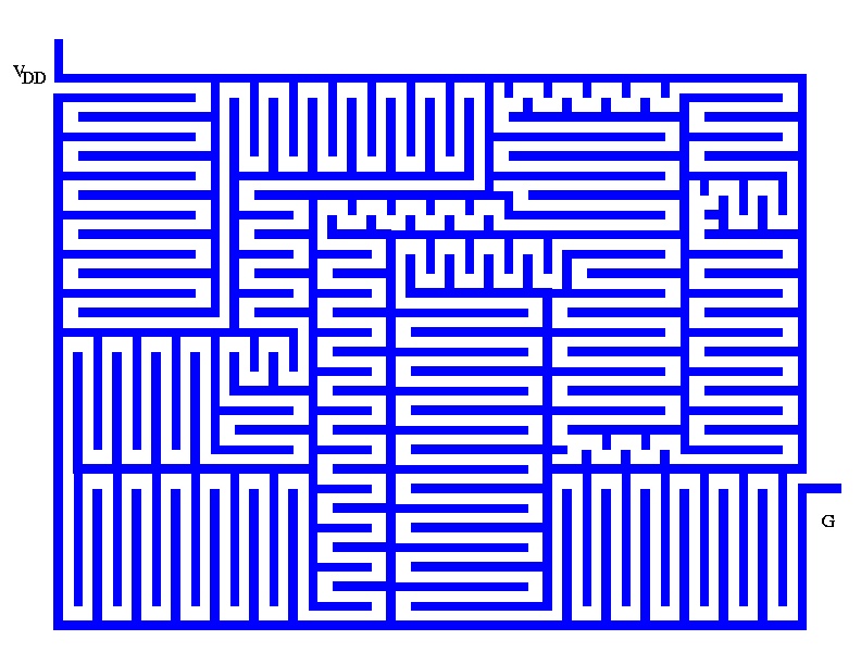
VLSI chips typically distribute VDD and ground voltages through
blue metal wires, in a pattern of interleaving feathery forms. This
form provides both VDD and ground nearby to every point on the
silicon. The computational action then consists of switching that VDD
and ground voltage through transistors in the red and green
layers. Here is a whimsical picture of the interleaving of VDD with
ground.
